Additional Lab Services
- Assembly Process Validation - Testing Applications
- Coating Thickness - Microsection
- Component Authenticity Verification - X-Ray, CSAM, Decapsulation, Plasma Decapsulation, SEM-EDS
- Consumer Product Testing - Testing Applications
- Counterfeit Component Analysis - X-Ray, CSAM, Decapsulation, Plasma Decapsulation, SEM-EDS
- Cross Section Analysis - Microsection
- Decapsulation of electronic devices with acid - Integrated Circuit Decapsulation
- Decapsulation of electronic devices with plasma - Microwave Plasma Decapsulation
- Dye and Pry Analysis - Testing Applications
- Failure Analysis - Testing Applications
- First Article Inspection - Testing Applications
- Lead-Free Quality and Reliability Testing - HALT/HASS, Environmental Chambers, Electromechanical Universal Tester
- Microsectioning
- Plating Thickness - Microsection, XRF
- Printed Circuit Board Thermal Analysis - TMA, TGA, DSC, Microsection, ICP-MS, SEM-EDS
- Product and Design Verification - Testing Applications
- Quality, Acceptance and Conformance Testing - Testing Applications
- Reliability and Durability Testing - HALT/HASS, Environmental Chambers
- Solderability - Testing Applications
- Structural Integrity Analysis - Microsection
- Supplier Surveillance Testing - Testing Applications
- Additional Lab Services Related Standards
Integrated Circuit Decapsulation
Decapsulation of epoxy packaged devices, such as integrated circuits (IC’s) or potted modules, uses heated acids (nitric and sulfuric) to remove the encapsulant to expose the internal components or silicon die within the package. Opening devices by decapsulation allows inspection of the die, interconnects and other features typically examined during failure analysis. Device failure analysis often relies on the selective etching of polymer encapsulants without compromising the integrity of the wire bonds and device layers.
Applications:
- Component Authenticity Verification
- Counterfeit Component Analysis
- Integrated Circuit Failure Analysis
Microwave Plasma Decapsulation
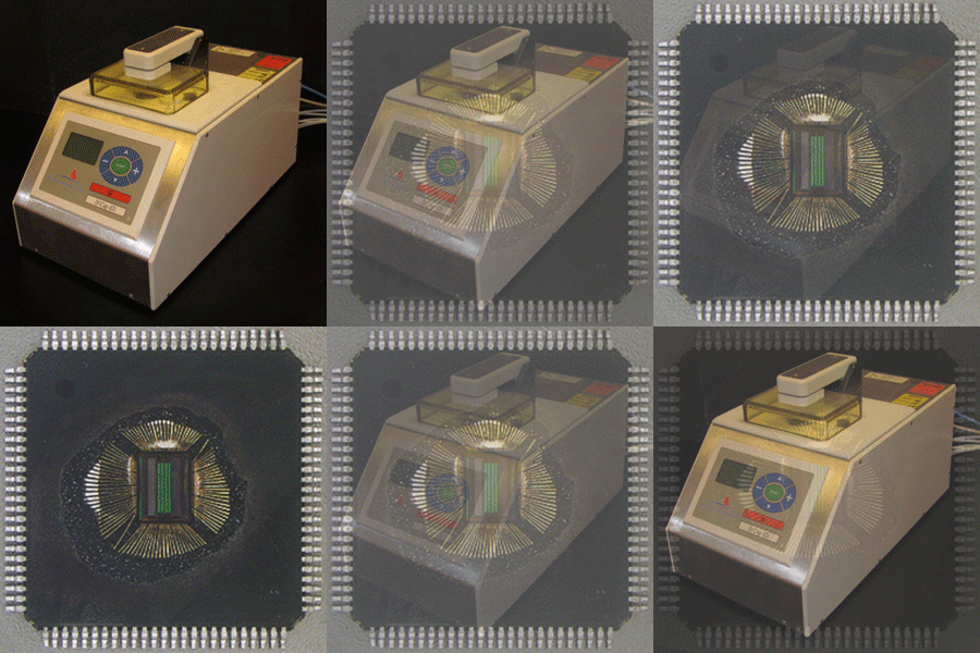
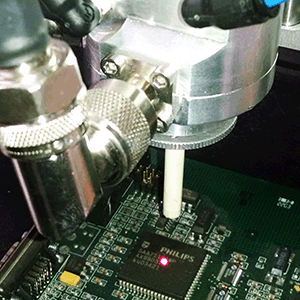
New integrated circuit packaging technologies have become a challenge to safely decapsulate with acid. Often the strength of the acid required to successfully remove the new high temperature epoxy encapsulants also destroys the bond wires and bond pads. Many cost sensitive designs use copper or copper plated bond wires. To address the limitations of acid decapsulation, Accolade has developed a microwave decapsulation system that selectively removes the encapsulant without harming any of the electrical structures of the part. With a small diameter atmospheric plasma source, selective encapsulant removal is possible and with closed loop process temperature control, the sample is quickly and safely decapsulated. Parts can also be decapsulated while still resident on the printed wiring board to aid in post decapsulation analysis.
Applications:
- Component Authenticity Verification
- Counterfeit Component Analysis
- Integrated Circuit Failure Analysis
Microsectioning
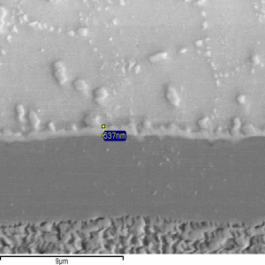
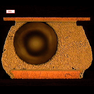
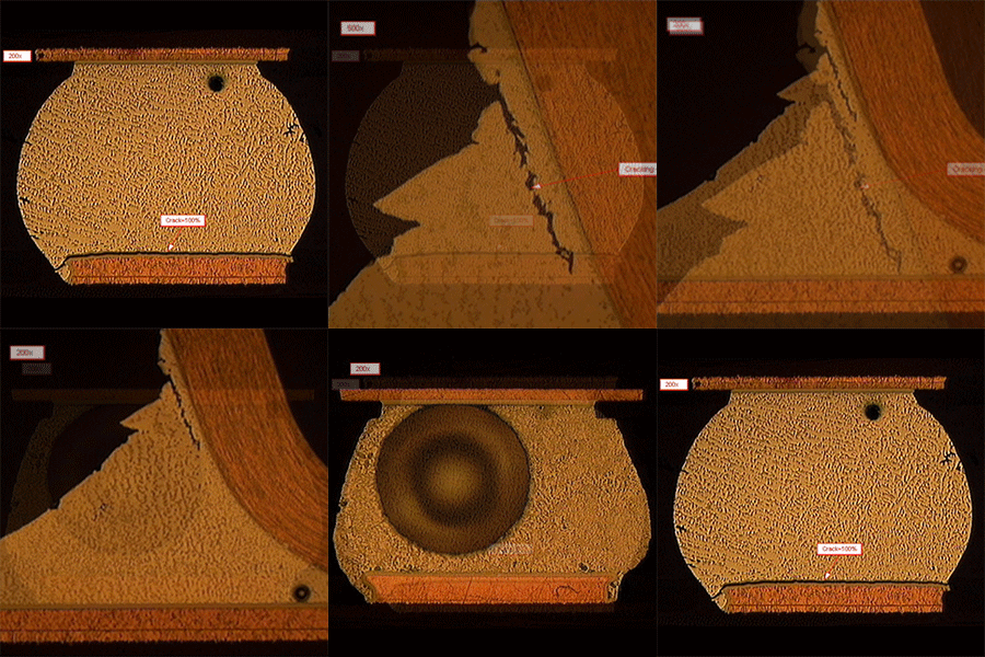
One of the most important and often overlooked methods to ensure electronic assembly solder process capability and the quality of printed wiring boards is to perform microsections. For the soldering process, external visual inspection (if possible) is a minimal and superficial technique to evaluate the soldering process. Beyond using a real time X-ray system to evaluate solder volume and voiding, a microsection of the solder attachments can provide more detail of the quality of the soldering process and when coupled with intermetallic measurement and elemental analysis with the SEM/EDS system, the quality of the solder process can be fully characterized and provide guidance for improvement of the soldering process. Printed wiring board suppliers are often selected by price and volume capability but the quality of the received material is usually evaluated for plated through hole inside diameters, twist, warp and external evaluation of silkscreen, soldermask and plating. Performing a microsection with acceptability per IPC-6012, IPC-6013 and your fabrication drawing provides the best evaluation of the printed wiring board fabrication process. When coupled with TMA thermal evaluation of the laminate CTE, Tg and time to delamination, the printed wiring board is fully characterized and while still compliance with IPC standards, different suppliers can be easily compared to find the highest quality supplier.
Applications:
- Coating Thickness
- Cross Section Analysis
- Intermetallic Layer Measurement
- Plating Thickness
- Printed Circuit Board Analysis
- Structural Integrity Analysis
Additional Lab Service Applications
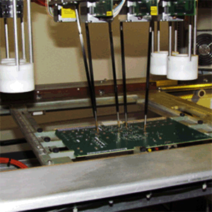
Accolade Engineering Solutions offers a variety of Testing Applications. Contact us today to discuss your testing needs with someone who can provide you with the expert knowledge to determine the right testing solution for you.
Applications:
- Assembly Process Validation
- Consumer Product Testing
- Dye and Pry Analysis
- Failure Analysis
- First Article Inspection
- Product and Design Verification
- Quality, Acceptance, and Conformance Testing
- Supplier Surveillance Testing
- And More...
Additional Lab Services Related Standards
- ASTM B263 "Standard Test Method for Determination of Cross-Sectional Area of Stranded Conductors"
- ASTM B735 "Standard Test Method for Porosity in Gold Coatings on Metal Substrates by Nitric Acid Vapor"
- EIA-364-53 "Nitric Acid Vapor Test, Gold Finish Test Procedure for Electrical Connectors and Sockets"
- IPC-4101 "Specification for Base Materials for Rigid and Multilayer Printed Boards"
- IPC-6012 "Qualification and Performance Specification for Rigid Printed Boards"
- IPC-6013 "Qualification and Performance Specification for Flexible Printed Boards"
- IPC-6016 "Qualification and Performance Specification for High Density Interconnect (HDI) Layers or Boards"
- IPC-9701 "Performance Test Methods and Qualification Requirements for Surface Mount Solder Attachments"
- IPC-CC-830 "Qualification and Performance of Electrical Insulating Compound for Printed Wiring Assemblies"
- IPC/J-STD-001 "Requirements for Soldered Electrical and Electronic Assemblies"
- IPC/J-STD-002 "Solderability Tests for Component Leads, Terminations, Lugs, Terminals and Wires"
- IPC/J-STD-003 "Solderability Tests for Printed Boards"
- IPC/J-STD-004 "Requirements for Soldering Fluxes"
- IPC/J-STD-005 "Requirements for Soldering Pastes"
- IPC-MF-150 "Metal Foil for Printed Wiring Applications"
- IPC-SM-840 "Qualification and Performance Specification of Permanent Solder Mask"
- IPC-TM-650, Method 2.1.1 "Microsectioning, Manual Method"
- IPC-TM-650, Method 2.1.1.2A "Microsectioning - Semi or Automatic Technique Microsection Equipment (Alternate)"
- IPC-TM-650, Method 2.1.10A "Visual Inspection for Undissolved Dicyandiamide"
- IPC-TM-650, Method 2.1.1E "Microsectioning"
- IPC-TM-650, Method 2.1.3A "Plated-Through Hole Structure Evaluation"
- IPC-TM-650, Method 2.1.5A "Surface Examination, Unclad and Metal Clad Material"
- IPC-TM-650, Method 2.1.6B "Thickness of Glass Fabric"
- IPC-TM-650, Method 2.1.8B "Workmanship"
- IPC-TM-650, Method 2.1.9 "Surface Scratch Examination Metal Clad Foil"
- IPC-TM-650, Method 2.2.10 "Hole Location and Conductor Location"
- IPC-TM-650, Method 2.2.18 "Determination of Thickness of Laminates by Mechanical Measurement"
- IPC-TM-650, Method 2.2.18.1 "Determination of Thickness of Metallic Clad Laminates, Cross-sectional"
- IPC-TM-650, Method 2.2.19.1 "Length, Width and Perpendicularity of Laminate and Prepreg Panels"
- IPC-TM-650, Method 2.2.1A "Mechanical Dimensional Verification"
- IPC-TM-650, Method 2.2.2B "Optical Dimensional Verification"
- IPC-TM-650, Method 2.2.4C "Dimensional Stability, Flexible Dielectric Materials"
- IPC-TM-650, Method 2.2.5A "Dimensional Inspections Using Microsections"
- IPC-TM-650, Method 2.2.6A "Hole Size Measurement, Drilled"
- IPC-TM-650, Method 2.2.7A "Hole Size Measurement, Plated"
- IPC-TM-650, Method 2.2.8 "Location of Holes"
- IPC-TM-650, Method 2.3.24 "Porosity of Gold Plating"
- IPC-TM-650, Method 2.3.24.1 "Porosity Testing of Gold Electrodeposited on a Nickel Plated Copper Substrate Electrographic Method"
- IPC-TM-650, Method 2.3.24.2 "Porosity of Metallic Coatings on Copper-Base Alloys and Nickel (Nitric Acid Vapor Test)"
- IPC-TM-650, Method 2.4.12A "Solderability, Edge Dip Method"
- IPC-TM-650, Method 2.4.13F "Solder Float Resistance Flexible Printed Wiring Materials"
- IPC-TM-650, Method 2.4.15A "Surface Finish, Metal Foil"
- IPC-TM-650, Method 2.4.35 "Solder Paste - Slump Test"
- IPC-TM-650, Method 2.4.44 "Solder Paste - Tack Test"
- IPC-TM-650, Method 2.4.46 "Spread Test, Liquid, Paste, or Solid Flux, of Flux Extracted from Solder Paste, Cored Wires or Preforms"
- IPC-TM-650, Method 2.4.47 "Flux Residue Dryness"
- IPC-TM-650, Method 2.4.48 "Spitting of Flux-Cored Wire Solder"
- IPC-TM-650, Method 2.4.36C "Rework Simulation, Plated-Through Holes for Leaded Components"
- IPC-TM-650, Method 2.4.38A "Prepeg Scaled Flow Testing"
- IPC-TM-650, Method 2.4.39A "Dimensional Stability, Glass Reinforced Thin Laminates"
- IPC-TM-650, Method 2.4.41.2A "Coefficient of Thermal Expansion – Strain Gage Method"
- JESD22-B105 "Lead Integrity Test"
- JESD22-B106 "Resistance to Soldering Temperature for Through-Hole Mounted Devices"
- JESD22-B107 "Marking Permanency"
- IPC-TM-650, Method 2.4.41.4 "Volumetric Thermal Expansion Polymer Coatings on Inorganic Substrates"
- MIL-A-28870 "General Specification for Assemblies, Electrical Backplane, Printed-Wiring"
- MIL-I-46058 "Insulating Compound, Electrical (For Coating Printed Circuit Assemblies)"
- MIL-P-50884 "General Specification for Printed Wiring Boards, Flexible or Rigid-Flex"
- MIL-PRF-31032 "General Performance Specification for Printed Circuit Boards/Printed Wiring Boards"
- MIL-PRF-55110 "General Performance Specification for Printed Wiring Boards, Rigid"
- MIL-DTL-83528C "General Specification for Gasketing Material, Conductive, Shielding Gasket, Electronic, Elastomer"
- MIL-STD-202 Method 208H "Solderability"
- MIL-STD-202 Method 209 "Radiographic inspection"
- MIL-STD-202 Method 210F "Resistance to soldering heat"
- MIL-STD-883 Method 2003.7 "Solderability"
- MIL-STD-883 Method 2008.1 "Visual and mechanical"
- MIL-STD-883 Method 2009.9 "External visual"
- MIL-STD-883 Method 2012.7 "Radiography"
- MIL-STD-883 Method 2013.1 "Internal visual inspection for DPA"
- MIL-STD-883 Method 2014 "Internal visual and mechanical"
- MIL-STD-883 Method 2016 "Physical dimensions"
- MIL-STD-883 Method 2017.7 "Internal visual (hybrid)"
- MIL-STD-883 Method 2018.3 "Scanning electron microscope (SEM) inspection of metallization"
- MIL-STD-883 Method 2030 "Ultrasonic inspection of die attach"
- MIL-STD-883 Method 2032.1 "Visual inspection of passive elements"
- MIL-STD-883 Method 2035 "Ultrasonic inspection of TAB bonds"
Copyright (c) 2014 accoladeeng.com. All rights reserved. | Design by FreeCSSTemplates.org.

